In Hsu's laboratory, students have access to state-of-the-art equipment for solution synthesis, nanomaterials characterization, fabrication and testing of solar cells, probing electronic and transport properties in devices. In addition, numerical simulation tools are available to model device behaviors.
Solution Synthesis:
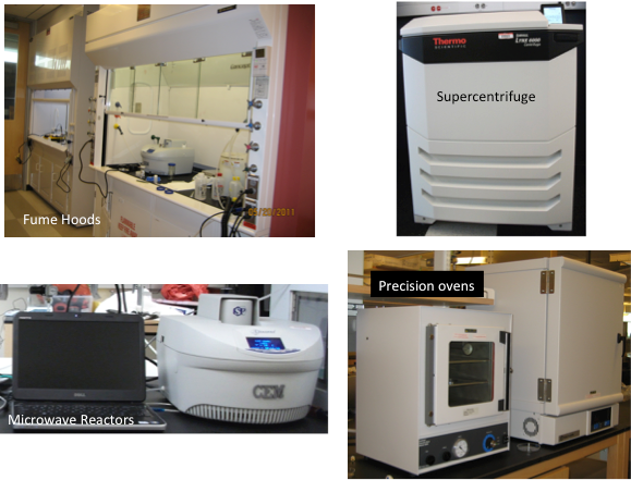
Hsu's laboratory has two fume hoods, two microwave reactors (CEM Discover SP), a stand-alone spin coater (Laurell), precision hot plates, a N2 glovebox (Terra Universal), a water purifier (Aqua Solutions), an ultrasonic bath (Branson), an ozone cleaner (Bioforce Nanosciences), a laminar flow hood (Labconco), precision microbalances and several digital programmable ovens and muffle furnaces. A 4L capacity centrifuge with maximum acceleration of 105,000 g (Sorvall Lynx 6000, Thermo Scientific) is used for sample purification and collection. Air and water sensitive materials can be handled in dry N2 atmosphere gloveboxes (Innovative Technology PureLab).
Materials Characterization:
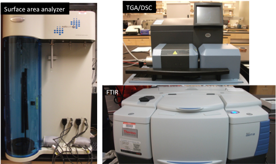
Sample characterization instruments include an FTIR spectrometer (Nicolet iS50) with a high sensitivity MCT-A detector, a UV-visible spectrometer capable of transmission and reflection measurements (Ocean Optics), and a fluorescence optical microscope with image capture and analysis capability (Leica DM2500). A dynamic light scattering system (Malvern ZEN3600) is used to measure nanoparticle size and zetapotential. A combination thermogravimetric analysis/differential scanning calorimetry instrument (TA Instruments Q600) can perform thermal analysis to probe phase transitions and materials stability up to 1500 °C. An atomic force microscope (Asylum MFP-3D) capable of contact, non-contact, electric force, scanning Kelvin probe, and scanning current imaging from room temperature to 300 °C in controlled atmosphere is also available. For enhanced performance, this microscope is situated in a vibration and sound isolation room. A low voltage benchtop transmission and scanning electron microscope (Delong LVEM5) with maximum resolution of 1.2 nm is used for rapid characterization of nanoscale samples. Notably, the low acceleration voltage allows us to distinguish high and low atomic number materials, and simultaneously image e.g. metal oxide nanoparticles surrounded by organic ligands.

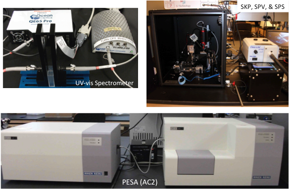
Electronic levels critically determine whether charges will transfer from one material to another or not. To measure the optical band gap of a semiconductor, we use UV-vis spectrometer (Ocean Optics); to measure the Fermi level (or work function), we have an electrostatic voltmeter (Monroe Electronics 244) and a scanning Kelvin probe system (Kelvin Technology SKP5050) capable of < 10 mV work function resolution and 0.4 µm position resolution. The most unique instrument in Hsu's lab is a photoelectron spectroscopy in air apparatus (RKI AC2) that can measure the ionization energy of materials in ambient (not solution, not UHV) environment. In addition, the SKP instrument is equipped with a tungsten-halogen light source to measure surface photovoltage as a function of intensity; with the additional monochrometer, surface photovoltage spectra can be obtained from 400nm to 1000nm.
For catalyst materials, the workhorse instrument is a Quantachrome Autosorb IQ surface area analyzer with Viton seals that can withstand corrosive gases like NO. The analyzer can measure the overall surface area (N2 BET physisorption) and catalytically active surface area for chemisorption of specific gases. In combination with FTIR and a mass spectrometer, we can also monitor the desorbed reaction intermediates and products as a function of temperature, i.e. temperature-programmed desorption.
Fabrication and Testing of Photovoltaic Devices
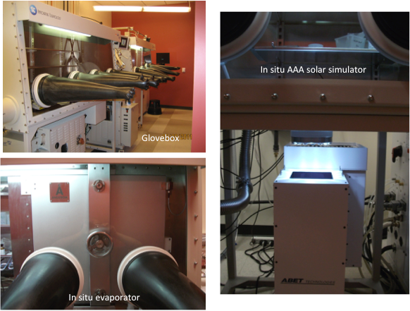
Two interconnected gloveboxes are used to fabricate and test solar cells. One of the glovebox is equipped with a spin coater (SCS G3P), microbalance, and hot plates for device fabrication; the other glovebox has an integrated thermal evaporator (Angstrom EvoVac).
Simulated One-sun Testing: The second glovebox is also equipped with in situ current-voltage testing of solar cell devices through a window using an AAA solar simulator (Abet) and a high-sensitivity sourcemeter (Keithley 2365A). The external quantum efficiency is measured using a NREL calibrated photodiode and a spectrometer (Horiba-Jobin Yvon Triax 180 with 100W tungsten-halogen light source).
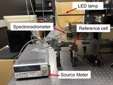
Indoor LED Testing: This setup up consists of a white-light LED lamp (MOICO Part number B07SSZ2YJ5), a NIST-calibrated reference cell (ID: NIST 1007), a low-noise source-meter (Keithley 2635B), and a spectroradiometer (Apogee instruments, PS-200). The LED lamp has ten adjustable brightness levels and five different nominal correlated color temperatures (CCTs). The reference cell is NIST calibrated and is a crystalline silicon solar cell with a nominal area of 20 mm × 20 mm with a KG5-filtered window (Newport part number FSQ-KG5) mounted in front to minimize the spectral mismatch factor between the reference cell and the organic PVs.
Device Physics Studies:
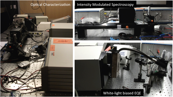
Impedance and intensity modulation spectroscopies are performed on a Zahner Electrik controlled intensity modulated photo spectroscopy (CIMPS) system. CIMPS includes an electrochemical workstation with a potentiostat for standard electrochemical impedance spectroscopy studies and a second high-power potentiostat for modulating light emitting diode intensity. The AC voltage bias frequencies range from sub-Hz to 8 MHz, with DC voltage bias and background light intensity (both white and specific wavelength) control. Capacitance-frequency measurements can be done with either the Zahner instrument or a precision LCR meter (Keysight E4980AL/032).Time-resolved charge extraction experiment is carried out with a 405 nm laser diode (SANYO, DL-5146-101S), a nanosecond time-resolved switch (AsamaLab, Solar Relay SR-05), a pulse generator (Stanford research systems, DG535), a wavefunction generator (Stanford research systems, DS345), and a an oscilloscope (Tektronix, DPO5104).
Device Simulations:
The Transfer Matrix Method (TMM) is used to investigate the photocurrent generation in organic solar cells by modeling all the optical effects (absorption, transmission, reflection, and interference) of a multilayer stack interacting with a normal incident planar wave of light. The optical electric field intensity profile is accurately calculated from TMM, which can be further interpreted into photo-generation in the solar cells. The Solar Cell Capacitance Simulator (SCAPS), developed at the University of Gent, is able to simulate the behavior of solar cells with and without illumination. Device structures with multiple semiconductor layers can be modeled with arbitrary doping profiles and energetic distributions. Moreover, SCAPS can simulate complex admittance at any frequency using small signal analysis technique. The output from TMM can be input into SCAPS to simulate a realistic photo-generation profile. We use the combined TMM-SCAPS to simulate solar cell current-voltage in dark and light, capacitance-frequency, capacitance-voltage, and external quantum efficiency to compare to experimental results. The numerical results provide insight into field and charge distribution inside the devices, as well as charge generation and recombination profiles.

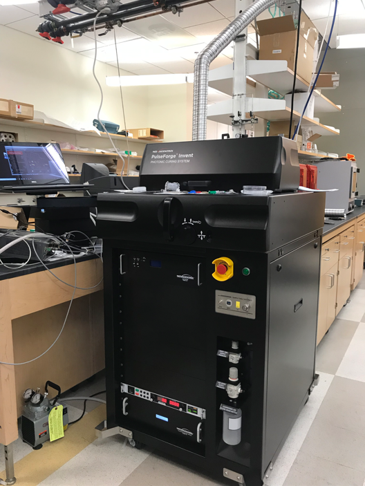
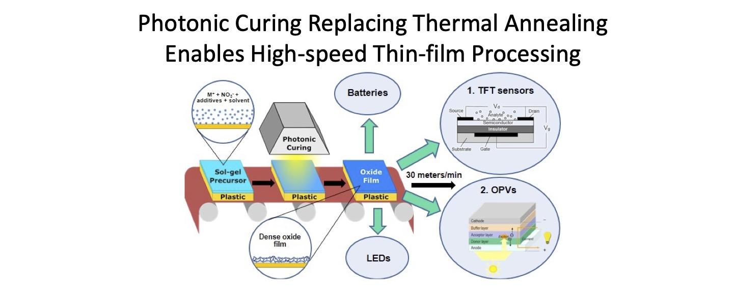
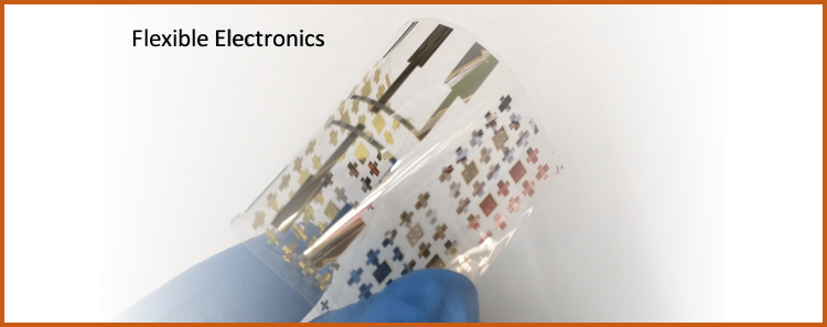
High Speed Photonic Processing of Thin Films:
Photonic curing uses intense pulses of broad-spectrum (200 – 1200 nm) light to process thin films on flexible substrates. The photonic curing system (NovaCentrix PulseForge® Invent) delivers short pulses (20 µs – 20 ms) of light from a xenon flash lamp at intensities up to 5 kW/cm2 to rapidly heat the thin films on top of a substrate. The substrate remains cool due to the low energy (<20 J/cm2) of the pulse. A calibrated bolometer is integrated into the system to measure the radiant energy of a pulse of light. The sample chuck (EX-1) includes a closed sample chamber with a quartz window for processing under different environments (air, vacuum, nitrogen).