
Researchers Pinpoint More Precise Method for Atomic-Level Manufacturing
Quantum computers have the potential to transform fields such as medicine, cybersecurity and artificial intelligence by solving hard optimization problems that are beyond the reach of conventional computing hardware.
But the technology to manufacture the devices on a large scale does not yet exist.
Researchers at UT Dallas have developed a technique that could remove one of the challenges to scaling the production of silicon quantum devices. The researchers outlined their method, which provides greater control and precision during the fabrication process, in a study published in the July 2020 issue of the Journal of Vacuum Science & Technology B. Silicon is the preferred material for the base of quantum devices because of its compatibility with conventional semiconductor technology.
The study’s corresponding author, Dr. Reza Moheimani, the James Von Ehr Distinguished Chair in Science and Technology and professor of systems engineering in the Erik Jonsson School of Engineering and Computer Science, received a $2.4 million Department of Energy grant in 2019 to develop technology for atomically precise manufacturing, the process of building new materials and devices atom by atom.
Moheimani’s team is addressing a range of challenges to quantum- device fabrication.
“Our latest work increases the precision of the fabrication process,” Moheimani said. “We’re also working to increase throughput, speed and reliability.”
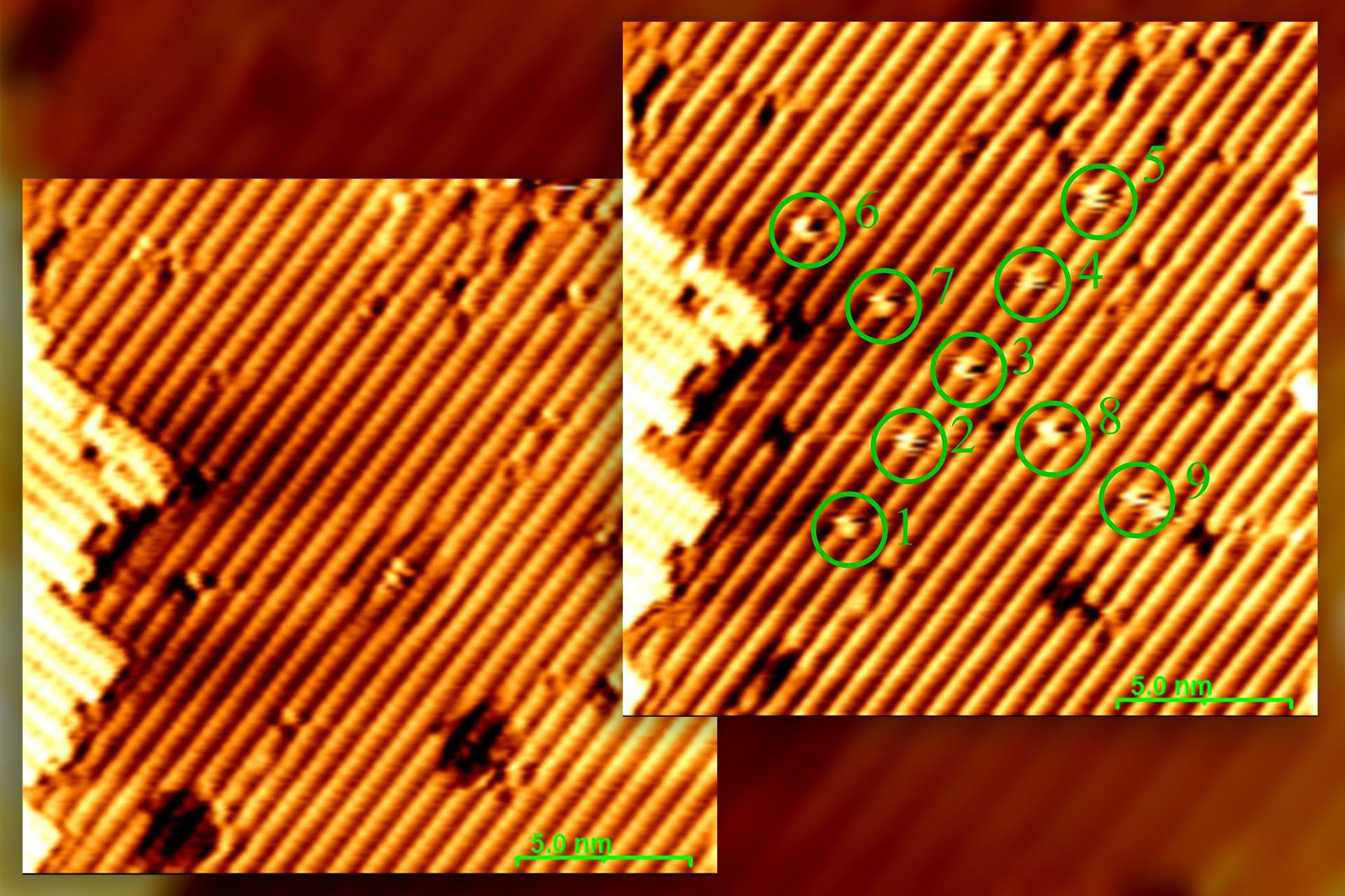
The researchers’ method for building a silicon-based qubit — or quantum bit, the basic unit of information in a quantum computer — starts with an atomically flat silicon surface coated with a layer of hydrogen, which prevents other atoms or molecules from getting absorbed into the surface. Next, researchers use a scanning tunneling microscope (STM), which features a probe with an atomically sharp tip, functioning as a microrobotic arm, to remove atoms of hydrogen selectively from the surface. The STM was designed for imaging atomic features on a surface; however, researchers also use the device to manipulate atoms in a mode called hydrogen depassivation lithography (HDL).
The researchers found that they could achieve higher precision by performing HDL in imaging mode, rather than the conventional lithography mode, with some adjustments to the voltage and a change to the STM’s feedback control system.
“We realized that we could actually use this method to remove hydrogen atoms in a controlled fashion,” Moheimani said. “This came as a surprise. It’s one of those things that happens during experiments, and you try to explain it and take advantage of it.”
– Kim Horner


